04 — The C-Forge: Carbon Processing Facility
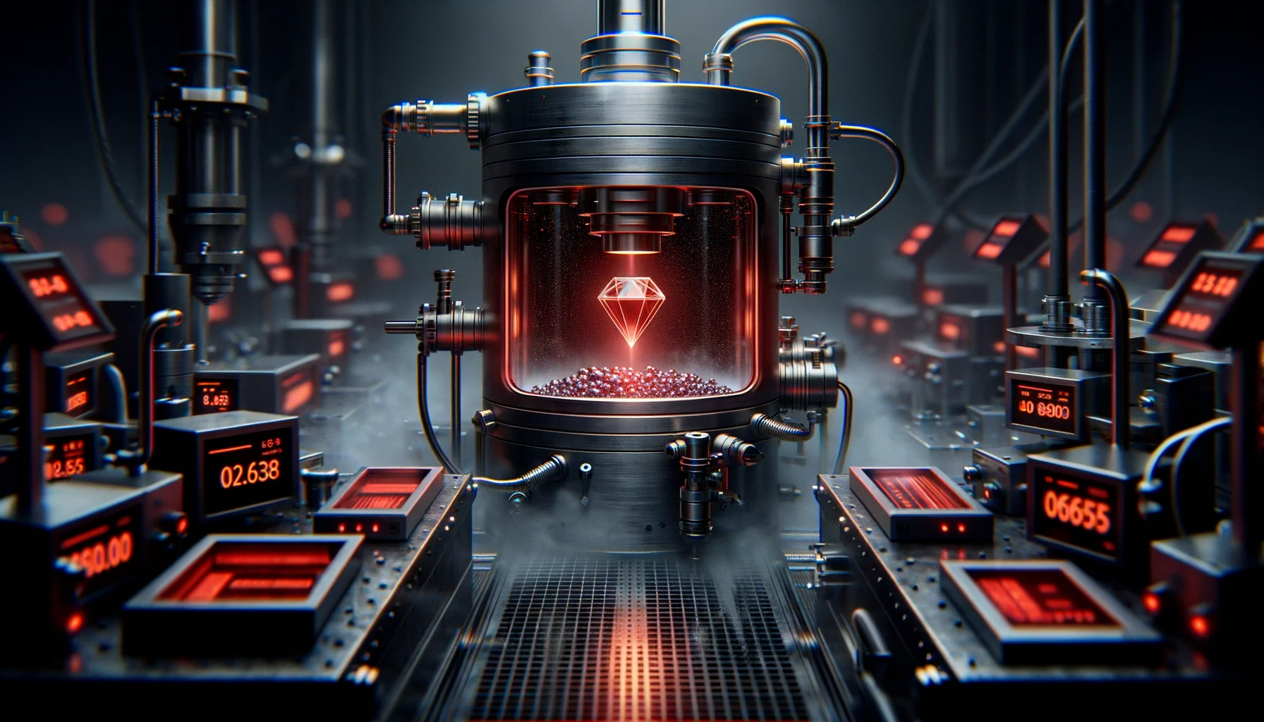
Carbon materials — diamond, graphene, carbon nanotubes — require fundamentally different processing from metals. Carbon cannot be melted conventionally; it sublimates. The C-Forge is a dedicated facility for CVD diamond growth, graphene deposition, and carbon nanotube synthesis, optimised for the purity and structural control that downstream applications demand.
Carbon is technically a non-metal, but graphene conducts electricity better than copper, and diamond is the best thermal conductor known. The material applications span computing substrates (Aetheric Sciences), hull coatings (Lorentz Aerospace), and heat spreaders (Stellar Furnace).
Facility Requirements
CVD diamond growth requires ultra-high vacuum (10−8 Torr minimum) and vibration isolation — any atmospheric contamination or mechanical disturbance disrupts crystal formation. The C-Forge operates in a Vapor Vacuum chamber with active vibration damping. Long diamond growth cycles (weeks to months) demand uninterruptible power supply.
Isotope-Controlled Feedstock
Standard industrial carbon is ~99% Carbon-12 and ~1% Carbon-13. The C-13 impurities scatter phonons, measurably reducing thermal conductivity in diamond. For thermal management and quantum computing substrates, isotopically enriched 12C feedstock improves performance. This enrichment is currently expensive and limited to research-grade quantities — scaling it to industrial volumes is an active development target.
Multi-Phase Processing
The C-Forge is designed to produce multiple carbon allotropes within a single facility by varying pressure, temperature, and deposition conditions. CVD for graphene, high-pressure high-temperature (HPHT) for diamond, and catalytic growth for nanotubes. The long-term target is a single chamber capable of switching between these regimes without breaking vacuum — reducing contamination from atmospheric exposure during inter-facility transfers.
For high-purity deposition, ion beam sources with magnetic mass analysis can select specific isotopes before deposition. This technique is established in semiconductor fabrication and is being adapted for carbon materials at larger substrate scales.
The Three Growth Zones
Atomic-Scale Quality Control (Research Target)
For next-generation applications — quantum computing substrates, single-photon sources — defect density must approach zero. The long-term research direction is massively parallel scanning probe arrays for defect detection and correction during growth. IBM's Millipede project demonstrated parallel STM tip arrays at the 1,000-tip scale; scaling to larger arrays is an open engineering problem. In-situ Raman spectroscopy provides real-time defect monitoring during CVD growth, enabling closed-loop process adjustment. This is a research-stage capability, not current production.